
 Contact
 Comment faire ses achats
Livraison
Guide d'achat
 Anglais
 149 b
149 b
Jusqu'à 30 jours pour les retours
Les clients ont également acheté

 /
/
 Livre de poche
 11.59
€
11.59
€





 /
Feuille
25.00
€
/
Feuille
25.00
€








 /
Livre de poche
29.80
€
/
Livre de poche
29.80
€





 /
Livre de poche
60.82
€
/
Livre de poche
60.82
€





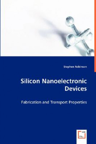
It is estimated that the scaling of conventional silicon MOSFETs will end around the year 2020. While this certainly does not preclude the use of silicon in future devices, it does require new thoughts on the types of practical devices that can be used in integrated circuits. Namely, those that reduce power and work at least partly on the principles of quantum mechanics (such as spintronic or tunneling devices) will tend to be favored. The research presented herein is based on the fabrication and transport properties of nanometer-scale devices in silicon. The most promising of these structures are nanowires fabricated with a scanning tunneling microscope (STM). These high-density nanowires display the low-temperature phenomena of weak localization and one-dimensional conduction. Long-term applications of such nanowires and derivative devices include alternatives to conventional CMOS transistors and very sensitive charge and/or spin-detection devices. In addition, focused ion beams (FIBs) have been used to directly and precisely implant ions in the hope that they may be used to contact nanodevices, but surface damage may preclude that possibility.


À propos du livre
Anglais

Offrez ce livre dès aujourd'hui
C’est simple
1 Ajouter au panier et choisir l'option Livrer comme cadeau à la caisse. 2 Nous vous enverrons un bon d'achat 3 Le livre arrivera à l'adresse du destinataireCeci pourrait également vous intéresser













 /
Livre de poche
223.68
€
/
Livre de poche
223.68
€



 /
Livre de poche
12.49
€
/
Livre de poche
12.49
€






Bonjour ! Je suis Libroamiko, votre conseiller littéraire.
Comment puis-je vous aider ?