
 Contact
 Hoe winkelen bij ons werkt
Bezorging
Winkelgids
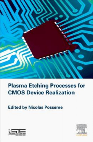
Plasma Etching Processes for CMOS Devices Realization
 Engels
 148 b
148 b
Tot 30 dagen retourrecht
Klanten kochten ook



 /
/
 Gebonden (paperback)
 26.94
€
26.94
€





 /
Gebonden (paperback)
28.15
€
/
Gebonden (paperback)
28.15
€



 /
Gebonden (paperback)
14.27
€
/
Gebonden (paperback)
14.27
€
 /
Gebonden (paperback)
28.95
€
/
Gebonden (paperback)
28.95
€


 /
Gebonden (paperback)
30.56
€
/
Gebonden (paperback)
30.56
€




Plasma Etching for CMOS Devices Realization addresses the ways in which plasma etch technologies are used to push the limits of semiconductor device fabrication. With the introduction of new materials and architectures, there are now unprecedented etching challenges, such as critical dimension control, profile control, and film damage at the atomic scale. This book addresses all the issues encountered in plasma etching processes for CMOS device realization. After an introduction of the different CMOS devices, the authors explore etch challenges and their associated solutions. Users will find this work to be the link between discovery of FEOL difficulties (today and tomorrow) and a precise understanding of the etch issues encountered in the microelectronics industry. Helps readers discover the master technology used to pattern complex structures involving various materialsExplores the capabilities of cold plasmas to generate well controlled etched profiles and high etch selectivities between materialsTeaches users how etch compensation helps to create devices that are smaller than 20 nm


Informatie over het boek
Engels
Categorieën

Geef dit boek vandaag nog cadeau
Dat gaat heel eenvoudig
1 Voeg het boek toe aan je winkelwagentje en selecteer Als cadeau bezorgen 2 Je krijgt van ons per omgaand een voucher 3 Het boek wordt bezorgd op het adres van de ontvangerDit vind je misschien ook interessant
 /
Gebonden (harde band)
39.01
€
/
Gebonden (harde band)
39.01
€


 /
Gebonden (paperback)
13.87
€
/
Gebonden (paperback)
13.87
€






 /
Gebonden (paperback)
70.68
€
/
Gebonden (paperback)
70.68
€




 /
Gebonden (paperback)
18.09
€
/
Gebonden (paperback)
18.09
€



 /
Gebonden (paperback)
15.48
€
/
Gebonden (paperback)
15.48
€


Hoi! Ik ben Libroamiko, je boekadviseur.
Hoe kan ik je helpen?